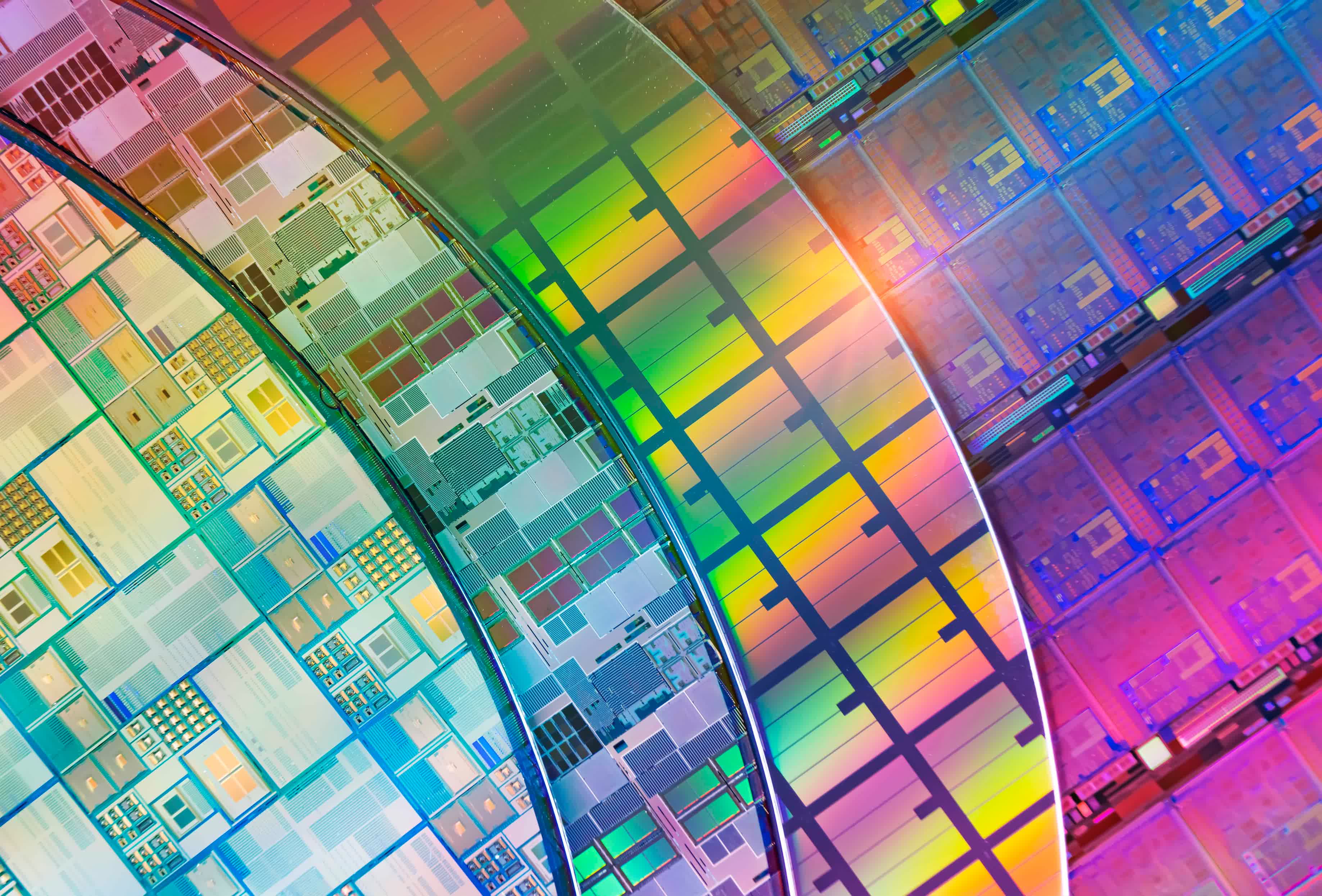
Forward-looking: TSMC has scheduled its performance-optimized N3P node to enter mass production in the second half of 2024, but it's not too soon to see what else the chipmaker has in store for the future. N3X, N2, N2P and A16 nodes, are coming in 2025 and 2026, bringing different strengths to the market, such as TSMC's first use of gate-all-around (GAA) nanosheet transistors in N2. Then there is A16, introduced only last month, that will be ideal for HPC products with complex signal routes and dense power delivery networks.
The competition to produce the world's most advanced chips is fierce, and TSMC's product roadmap promises that the battle for supremacy will be intense. First, its performance-optimized N3P node is coming, set to enter mass production in the second half of 2024 and will be the company's most advanced node for a while.
Next year, however, TSMC will introduce two production nodes that will enter high-volume manufacturing in the second half of 2025, promising to accelerate the advantages of N3P. These nodes are N3X, a 3nm-class process, and N2, a 2nm-class process.
N3X is tailored for high-performance computing applications, with a maximum voltage of 1.2V. According to research compiled by AnandTech, N3X chips can either reduce power consumption by 7% by lowering Vdd from 1.0V to 0.9V, increase performance by 5%, or increase transistor density by around 10%.
N2 uses gate-all-around (GAA) nanosheet transistors – a first for TSMC – and features exceptional low Vdd performance that is designed for mobile and wearable applications. In addition, N2's ultra-thin stacked nanosheets deliver a new level of energy efficient computing for HPC, TSMC says. Backside power rail will also be added to boost performance even further.
N2 technology will come with TSMC NanoFlex, a design-technology co-optimization that provides designers with flexibility in N2 standard cells, with short cells emphasizing small area and greater power efficiency, and tall cells maximizing performance. Customers are able to optimize the combination of short and tall cells within the same design block.
In 2026, TSMC will introduce two more nodes: N2P (2nm-class) and A16 (1.6nm-class).

N2P is expected to deliver a 5% - 10% lower power or a 5% - 10% higher performance compared to the original N2. However, contrary to prior announcements, N2P will not incorporate a backside power delivery network, using conventional power delivery mechanisms instead. This means the integration of such advanced power delivery will shift to future generation nodes, including A16.
TSMC announced A16 last month. A16 will combine TSMC's Super Power Rail architecture with its nanosheet transistors, improving logic density and performance by dedicating front-side routing resources to signals, making A16 ideal for HPC products with complex signal routes and dense power delivery networks. Compared to TSMC's N2P process, A16 will provide 8-10% speed improvement at the same Vdd (positive power supply voltage), 15-20% power reduction at the same speed, and up to 1.10X chip density improvement for data center products.

