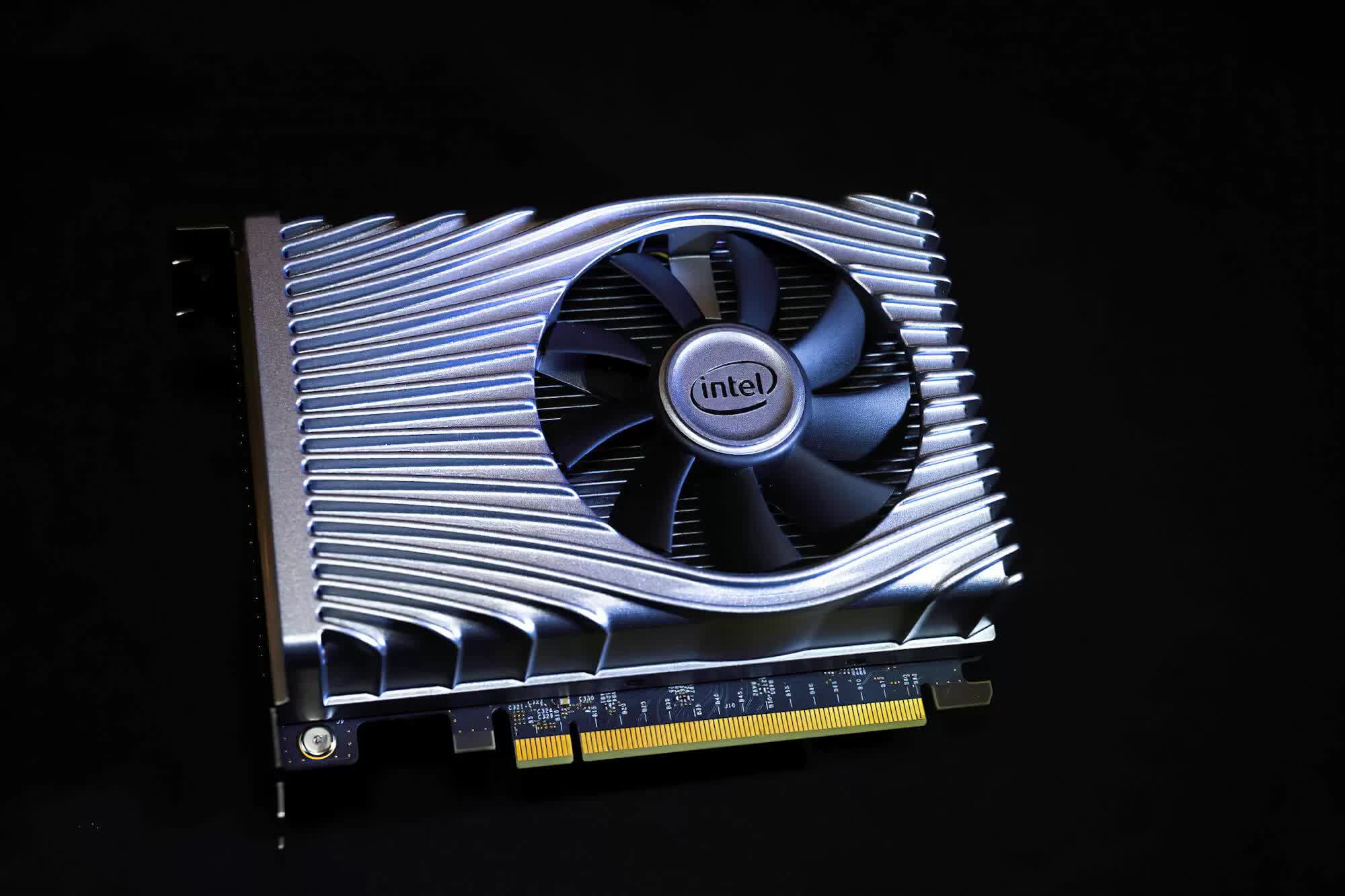
Will history repeat itself? Intel's setting out to make a name for itself in the discrete GPU space with its upcoming Xe-HP GPU lineup. We look at Project Larrabee - the last time Intel tried making a graphics card - to understand how things might turn out.
AMD just took the CPU performance crown, new consoles look like minimalist PCs, and Intel's working on a flagship GPU based on the Xe architecture, set to compete with Ampere and Big Navi. 2020 has been a topsy-turvy year for a whole lot of reasons. But even then, an Intel graphics card? You'd be forgiven for chalking it off as yet another 2020 oddity, but that's where things get interesting.
Raja Koduri's baap of all isn't actually Intel's first attempt at a desktop-grade discrete GPU. Fourteen years ago, the CPU maker started work on Project Larrabee, a CPU/GPU hybrid solution touted to revolutionize graphics processing. Larrabee terrified the competition to the point that AMD and Nvidia briefly considered a merger.
What happened then? Three years of development, an infamous IDX demo, and then... nothing. Project Larrabee quietly shuffled off stage, and some of its IP was salvaged for Xeon Phi, a many-core accelerator for HPC and enterprise workloads. Intel went back to integrating small, low-profile iGPUs with its processors.
What happened to Larrabee? What went wrong? And why haven't we seen a competitive Intel GPU in over a decade? With the Xe HP discrete GPU set to launch next year, we're looking today at the last time Intel tried to build a graphics card.
Intel Larrabee: What Was It?
While Intel started work on Project Larrabee sometime in 2006, the first official tidbit came at the Intel Developer Forum (IDF) 2007 in Beijing. VMWare CEO Pat Gelsinger, then a Senior VP at Intel, had this to say:
"Intel has begun planning products based on a highly parallel, IA-based programmable architecture codenamed "Larrabee." It will be easily programmable using many existing software tools, and designed to scale to trillions of floating point operations per second (Teraflops) of performance. The Larrabee architecture will include enhancements to accelerate applications such as scientific computing, recognition, mining, synthesis, visualization, financial analytics and health applications."
A highly parallel, programmable architecture, capable of scaling to teraflops of performance. Gelsinger's statement would've been a perfect description of any Nvidia or AMD GPU on the market, except for one key point: Larrabee was programmable and IA (x86)-based.
This meant that its cores were functionally similar to general-purpose Intel CPU cores, unlike the fixed-function shader units found in GPUs. Larrabee rendered graphics, but it wasn't a GPU in the conventional sense. To understand exactly how Larrabee worked, it's a good idea to first look at how conventional GPUs operate.
A GPU, a CPU, or Something Else? How Larrabee Worked
Nvidia and AMD GPUs are massively parallel processors with hundreds (or thousands) of very simple cores that handle fixed-function logic. These cores are limited in terms of what they can do, but parallelization massively speeds up those particular graphics workloads.
GPUs are very good at rendering graphics. But the fixed function nature of their shader cores made it difficult to run non-gaming workloads on them. This meant that game technology innovations were often held in check by graphics hardware capabilities.
New DirectX or OpenGL graphics feature sets required entirely new hardware designs. Tessellation, for instance, is a DirectX 11 feature that dynamically increases the geometric complexity of on-screen objects. AMD and Nvidia needed to implement fixed-function tessellation hardware into their Fermi and Terascale 2 cards to leverage this new capability.
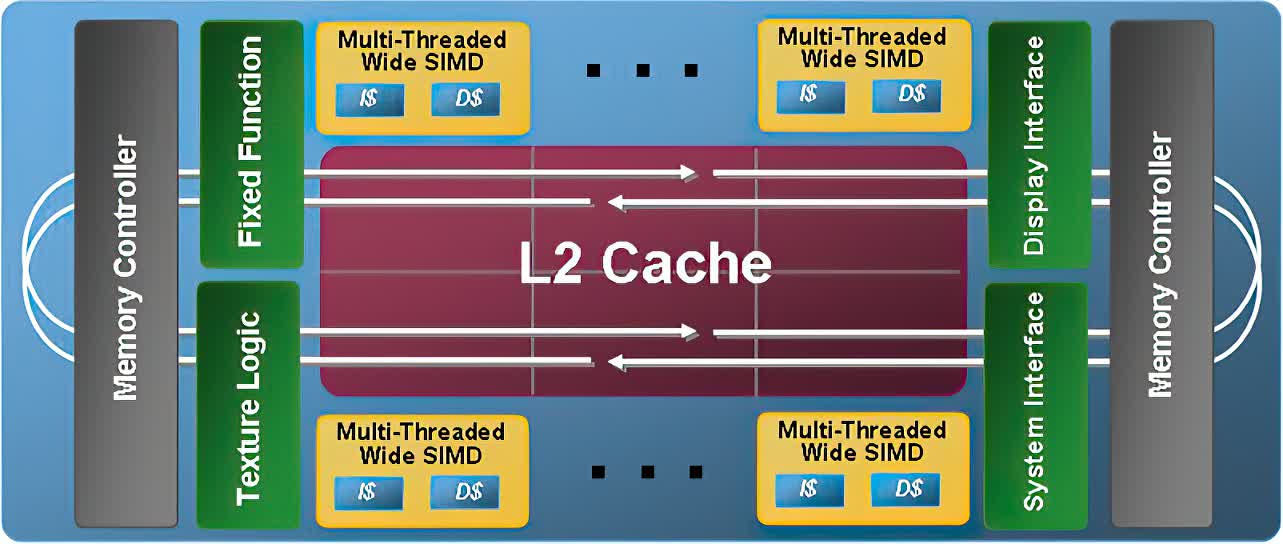
Larrabee, in contrast, was built out of a large number of simplified x86-compliant CPU cores, loosely based on the Pentium MMX architecture. Unlike GPUs, CPUs feature programmable, general-purpose logic. They can handle just about any kind of workload with ease. This was meant to be Larrabee's big trump card. A general-purpose, programmable solution like Larrabee could do tessellation (or any other graphics workload) in software. Larrabee lacked fixed function hardware for rasterization, interpolation, and pixel blending. In theory, this'd incur a performance penalty. However, Larrabee's raw throughput, the flexibility of those x86 cores, and Intel's promised game-specific drivers were meant to make up for this.
Developers wouldn't be limited by what functions graphics hardware could or couldn't perform, opening the door to all kinds of innovation. In theory, at least, Larrabee offered the flexibility of a many-core CPU, but with Teraflop-level raw throughput that matched top 2007 GPUs. In practice, however, Larrabee failed to deliver. Higher-core configurations scaled poorly. They struggled to match, let alone beat AMD and Nvidia GPUs in conventional raster workloads. What exactly led Intel down this technological dead-end?
Costs and Philosophy: The Rationale Behind Larrabee
Corporations like Intel don't invest billions of dollars towards new paradigms without a long-term strategic goal in mind. By the mid-2000s, GPUs were gradually becoming more flexible. ATI debuted a unified shader architecture with the Xbox 360's Xenos GPU. Terascale and Tesla (the Nvidia GeForce 200 series) brought unified shaders to the PC space. GPUs were getting better at generalized compute workloads, and this concerned Intel and other chip makers. Were GPUs about to make CPUs redundant? What could be done to stem the tide? Many chipmakers looked to multi-core, simplified CPUs as a way forward.
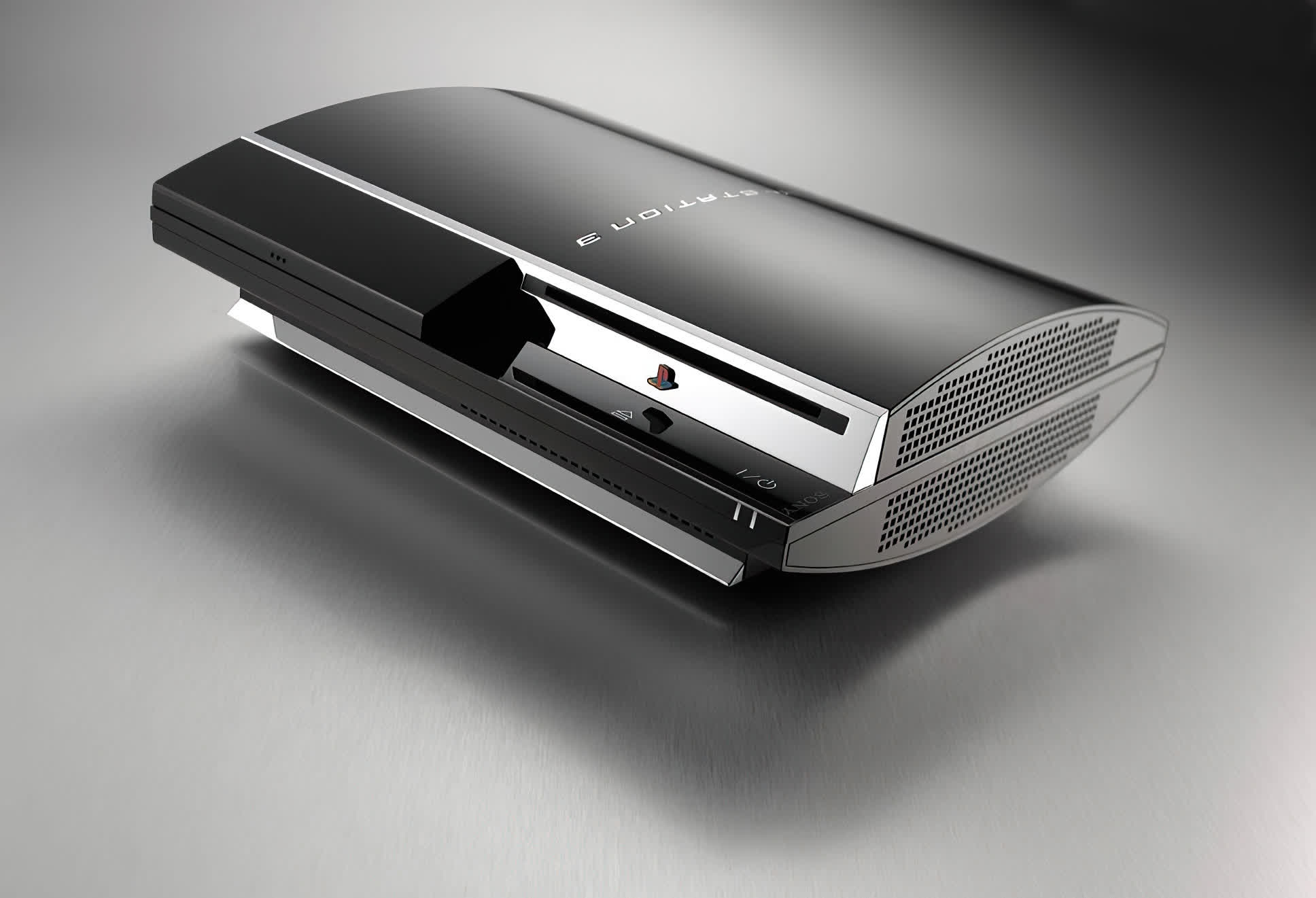
The PlayStation 3's Cell processor is the best-known outcome of this line of thought. Sony engineers initially believed that the eight-core Cell would be powerful enough to handle CPU and graphics workloads all by itself. Sony realized its mistake late into the PlayStation 3's development cycle, tacking on the RSX, a GPU based on Nvidia's GeForce 7800 GTX. Most PlayStation 3 games relied heavily on the RSX for graphics workloads, often resulting in worse performance and image quality compared to the Xbox 360.
Cell's SPUs (synergistic processing units) were used by some first-party studios to help with graphics rendering – notably in Naughty Dog titles like The Last of Us and Uncharted 3. Cell certainly helped, but it clearly wasn't fast enough to handle graphics rendering on its own.
Intel thought along similar lines with Larrabee. Unlike Cell, Larrabee could scale to 24 or 32-core designs. Intel believed that the raw amount of processing grunt would let Larrabee compete effectively with fixed-function GPU hardware.
Intel's graphics philosophy wasn't the deciding factor, though. It was cost. Designing a GPU from scratch is extremely complicated, time-consuming, and expensive. An all-new GPU would take years to design and cost Intel several billion dollars. Worse, there was no guarantee that it'd beat or even match upcoming Nvidia and AMD GPU designs.
Larrabee, in contrast, repurposed Intel's existing Pentium MMX architecture, shrunk down to the 45nm process node. Reusing a known hardware design meant Intel could (in theory) get a working Larrabee design out on the market faster. It would also make it easier to set and monitor performance expectations. Larrabee ended up burning a several-billion-dollar hole in Intel's pockets. However, cost-effectiveness was, ironically, one of its initial selling points. Larrabee looked revolutionary on paper. Why did it never take off?
What Went Wrong with Larrabee?
Larrabee was a great idea. But execution matters just as much as innovation. This is where Intel failed. Throughout its 4-year lifecycle, Larrabee was plagued by miscommunication, a rushed development cycle, and fundamental issues with its architecture. In retrospect, there were red flags right from the beginning.
Gaming wasn't even mentioned as a use case in Larrabee's initial announcement. However, almost immediately after, Intel started talking about Larrabee's gaming capabilities, setting expectations sky-high. In 2007, Intel was several times larger than Nvidia and AMD put together. When Intel claimed Larrabee was faster than existing GPUs, it was taken as a given, considering their talent pool and resource budget.
Larrabee gaming expectations were hyped even further when Intel purchased Offset Software, months after buying the Havok physics engine. The studio's first game, Project Offset, was demoed in 2007 and showcased unprecedented visuals. Unfortunately, nothing came out of the Offset Software purchase. Intel shuttered the studio in 2010, around the time it put Larrabee on hold.
Intel's gaming performance estimates ran counter to the hype. A 1GHz Larrabee design, with somewhere between 8 to 25 cores, could run 2005's F.E.A.R. at 1600x1200 at 60 FPS. This wasn't impressive, even by 2007 standards. By estimating Larrabee's performance at 1GHz, instead of the expected shipping frequency, Intel undersold the part's gaming capabilities. In a PC Pro article, an Nvidia engineer scoffed that a 2010 Larrabee card would deliver 2006 levels of GPU performance.
Who was Larrabee for? What was it good at doing? How did it stack up to the competition? The lack of clarity on Intel's part meant that none of these questions were ever answered. Communication wasn't the only issue, however. As development was underway, Intel engineers discovered that Larrabee had serious architectural and design issues.
The GPU that Couldn't Scale
Each Larrabee core was based on a tweaked version of the low-performance Pentium MMX architecture. Per-core performance was a fraction of Intel's Core 2 parts. However, Larrabee was supposed to make up for this by scaling to 32 cores or more. It was these big Larrabee implementations – with 24 and 32 cores – that Intel compared to Nvidia and AMD GPUs.
The problem here was getting the cores to talk to each other and work efficiently together. Intel opted to use a ring bus to connect Larrabee cores to each other and to the GDDR5 memory controller. This was a dual 512-bit interconnect with over 1 TB/s of bandwidth. Thanks to cache coherency and a surfeit of bandwidth, Larrabee scaled reasonably well... until you hit 16 cores.
One of the key drawbacks to the ring topology is that data needs to pass through each node on its way. The more cores you have, the greater the delay. Caching can alleviate the issue, but only to a certain extent. Intel tried to solve this problem by using multiple ring buses in its larger Larrabee parts, each serving 8-16 cores. Unfortunately, this added complexity to the design and did little to alleviate scaling issues.
By 2009, Intel was in a catch-22: 16-core Larrabee designs were nowhere near as fast as competing Nvidia and AMD GPUs. 32 and 48-core designs could close the gap, but at twice the power consumption and at an immense added cost.
IDF 2009 and Quake 4 Ray-Tracing: Shifting the Conversation
In September 2009, Intel showcased Larrabee running an actual game, with real-time ray-tracing enabled, no less. This was supposed to be Larrabee's watershed moment: in-development silicon running Quake 4 with ray-tracing enabled. Here was Larrabee hardware powering through a real-game with lighting tech that was simply not possible on GPU hardware at that time.
While the Quake 4 demo generated media buzz and stoked discussion about real-time ray-tracing in games, it skipped over far more serious issues. The Quake 4 ray-tracing demo wasn't a conventional DirectX or OpenGL raster workload. It was based on a software renderer that Intel had earlier showcased running on a Tigerton Xeon setup.
The IDF 2009 demo showed that Larrabee could run a complex piece of CPU code fairly well. But it did nothing to clear questions about Larrabee's raster performance. By attempting to shift the conversation away from Larrabee's rasterization performance, Intel inadvertently drew attention back to it.
Just three months after the IDF demo, Intel announced that Larrabee was being delayed and that the project was getting downsized to a "software development team."
A few months later, Intel pulled the plug entirely, stating that they "will not bring a discrete graphics product to the market, at least in the short term." This was the end of Larrabee as a consumer product. However, the IP that the team built would continue in a new, enterprise avatar: the Xeon Phi.
Xeon Phi and the Enterprise Market: Coming Full Circle
The strangest part of the Larrabee saga is that Intel actually delivered on all of its initial promises. Back in 2007, when Larrabee was first announced, Intel positioned it as a bold, new offering for the enterprise and HPC markets: a highly-parallel, many-core, programmable design that could crunch numbers far faster than a conventional CPU.
In 2012, Intel announced its Xeon Phi coprocessor, designed to do exactly that. The first-generation Xeon Phi parts even came with PCIe out: it was a die-shrunk, optimized Larrabee in all but name. Intel continued to sell Xeon Phi coprocessors to enterprise and research clients until last year, before quietly killing off the product line.
Today, with Intel working again on a discrete GPU architecture, there are definitely lessons to be learned here, along with hints about Intel's long-term strategy with Xe.
Learning from Larrabee: Where Does Xe Go From Here?
Intel Xe is fundamentally different from Larrabee. For starters, Intel now has a lot of experience building and supporting modern GPUs. Ever since the HD 4000, Intel's invested considerable resources towards building capable GPUs, supported by a fairly robust software stack.
Xe builds on top of over a decade's experience, and it shows. The Intel Xe-LP GPU in top-end Tiger Lake configurations matches or beats entry-level discrete GPUs from AMD and Nvidia. Xe manages this, even when it has to share 28W of power with four Tiger Lake CPU cores. Inconsistent performance across games indicates that Intel's driver stack still needs some work. But by and large, Xe-LP holds its own against entry-level AMD and Nvidia offerings. Xe (and previous-generation Intel iGPUs) make use of a number of Larrabee innovations, including tile-based rendering and variable SIMD width: the R&D Intel put towards Larrabee didn't go to waste.
While Xe-LP proves that Intel can build a decent, efficient mobile graphics chip, the real question here is how Xe-HPG, the discrete desktop variant, will perform. Efficient, low-power GPUs don't always scale up into 4K gaming flagships. If that were the case, Imagination's supremely efficient PowerVR chips would be giving Nvidia and AMD a run for their money.
Based on what Intel's said so far, Xe-HPG should offer feature parity with modern AMD and Nvidia GPUs. This means hardware ray-tracing and full support for other aspects of the DirectX 12 Ultimate feature-set. Intel also talked about using MCM to scale performance on upcoming Xe parts. By packing multiple GPU dies on a single MCM package, future Xe designs could scale performance well beyond what we're seeing with Ampere and Big Navi today.
However, the competition isn't standing still. AMD's already leveraging MCM in its chiplet-based Zen CPU design, while Nvidia's next-generation "Hopper" GPUs are also expected to use the technology to maximize performance.
The question, then, isn't really whether or not Intel can build a great discrete GPU – it probably can. But in a rapidly evolving hardware space, what matters is how Xe-HPG will stack up against upcoming Nvidia and AMD GPUs.
Intel has lessons to learn here from Larrabee: clear communication and expectation management are critical. Moreover, Intel needs to evolve and stick to realistic development timelines. A two-year wait could set Xe back a generation or more. And lastly, they need to focus on developing a mature driver stack: a powerful Xe-HP GPU won't count for much if it's held back by spotty drivers.
Is Xe going to usher in a new era of Intel graphics dominance? Or will it go the way of Larrabee? We'll only know for sure in the months to come when the "baap of all" makes it to market.
